USB-C 3.1 Breakout Board
Official Store Deal
Expert Analysis Overview
The USB 3.1 Type-C Connector 16 Pin Test PCB Board is a fundamental component for electronics technicians and hobbyists, enabling direct access to core USB-C data and power lines for repair, prototyping, and custom integration. This small adapter board addresses the common challenge of interfacing with the compact and intricate USB-C standard, providing a simplified, robust connection point for experimentation and practical application. It is a critical tool for anyone working with modern electronics that utilize the ubiquitous Type-C interface, offering a bridge between complex surface-mount components and more accessible through-hole wiring techniques.
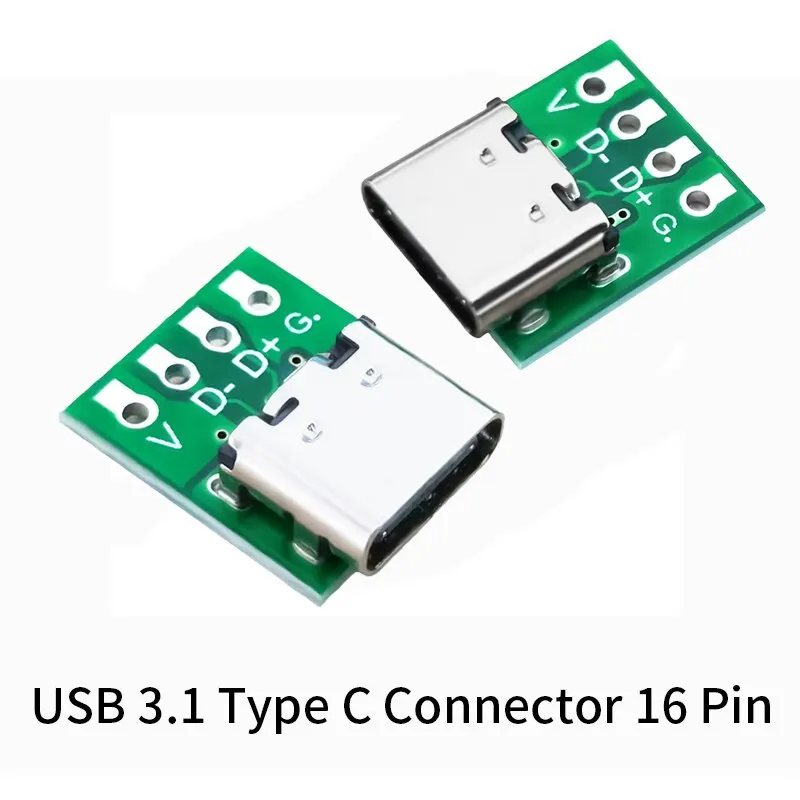
This breakout board features a single USB Type-C female connector, meticulously soldered onto a compact green PCB. The connector itself is designed for USB 3.1 specifications, though the breakout pads primarily expose the essential USB 2.0 data lines (D+, D-), power (V), and ground (G). This configuration makes it ideal for applications where high-speed USB 3.x data transfer is not the primary requirement, focusing instead on reliable power delivery and basic data communication.
The exposed pads are clearly labeled: 'V' for VBUS (voltage bus), 'D-' for Data Minus, 'D+' for Data Plus, and 'G.' for Ground. These labels are crucial for correct wiring, preventing potential damage to connected devices. The board's design prioritizes clarity and ease of use for manual soldering, a significant advantage over attempting to solder directly to a bare USB-C connector's tiny pins.
Compared to directly soldering wires onto a USB-C port, which is often a delicate and frustrating task due to the small pin pitch and fragile nature of the connector, this breakout board offers a stable, pre-mounted interface. This significantly reduces the risk of short circuits or damaged pins during assembly, streamlining the repair or prototyping process considerably. It simplifies connection.
While the board exposes the USB 3.1 Type-C connector, the breakout pads specifically cater to the USB 2.0 differential data pair (D+ and D-) and the VBUS/GND lines. This means that for applications requiring the full bandwidth of USB 3.1 (which includes additional SuperSpeed data pairs), this particular board would serve as a power and USB 2.0 data interface. For many embedded systems, charging solutions, or basic data logging, USB 2.0 speeds are entirely sufficient.
The VBUS and Ground pads are robust, designed to handle the typical current draw associated with USB power delivery. It is important to remember that while USB-C can support Power Delivery (PD) up to 100W, this specific breakout board does not include the necessary CC (Configuration Channel) pins or power negotiation circuitry. Its function is to provide direct access to the standard 5V VBUS line and ground, suitable for charging low-power devices or powering microcontrollers.
Imagine integrating a USB-C charging port into a custom enclosure for a portable device. This board provides a clean, easily mountable solution for power input, far superior to a flimsy micro-USB or mini-USB connection. The connection is stable. This capability extends the lifespan of custom projects by utilizing a modern, reversible, and robust connector standard.
The physical dimensions of the PCB are remarkably compact, measuring approximately 12mm by 13.8mm. This miniature footprint allows for integration into tight spaces, a common requirement in modern electronics design and repair. The through-hole pads are generously sized for their context, facilitating easier soldering for individuals with varying levels of experience.
The board's small size makes it an excellent candidate for repairing devices where the original USB-C port has been physically damaged. Instead of replacing an entire, often complex, mainboard, a technician can carefully desolder the damaged port and wire this breakout board into the existing VBUS, D+, D-, and GND traces. This approach can save significant repair costs and extend the life of valuable equipment.
Unlike larger, more complex USB-C development boards that might include additional components like resistors for CC pin configuration or voltage regulators, this board strips down the functionality to its bare essentials. This minimalist design reduces potential points of failure and keeps the cost exceptionally low, making it an accessible component for bulk purchases or single-use repairs. It is a simple, effective solution.
The USB-C connector itself is a metal-shielded component, offering decent mechanical durability against repeated insertions and removals. The soldering of the connector to the PCB appears solid, minimizing the risk of the connector detaching under normal stress. The green PCB material is standard FR-4, providing adequate rigidity for its size.
For applications where the connector will experience frequent mating cycles, proper strain relief on the connected wires is always recommended. While the connector is robust, excessive pulling or bending on the attached cable can still stress the solder joints or the PCB itself. A well-designed enclosure or cable clamp can significantly enhance the long-term reliability of the integrated solution.
Compared to the often fragile surface-mount USB-C ports found directly on consumer electronics, this breakout board offers a more repair-friendly interface. The larger through-hole pads are inherently more forgiving for manual soldering and can withstand more mechanical stress than tiny surface-mount pads. This makes it a more durable option for DIY projects. The board holds up well.
This USB-C breakout board is an indispensable tool for anyone involved in electronics repair, especially for devices with damaged charging or data ports. The cost of replacing a mainboard due to a faulty USB-C port can be prohibitive, often making a device uneconomical to repair. This small board offers a cost-effective alternative, allowing technicians to restore functionality at a fraction of the price.
Beyond repair, it is invaluable for prototyping. When developing a new circuit that needs USB-C connectivity for power or basic data, this board provides an immediate and easy way to integrate the connector without needing to design a custom PCB for just the port. It accelerates development cycles, allowing engineers and hobbyists to focus on their core circuit design rather than connector integration challenges.
Consider a scenario where a custom IoT device requires a modern power input. Using this breakout board, a developer can quickly add a USB-C port, ensuring compatibility with contemporary chargers and cables. This future-proofs the power input compared to older, less convenient connector types. The board provides essential capability.
This board offers exceptional value. Its low cost, combined with its ability to save expensive equipment from being discarded, makes it a highly attractive component for any electronics workbench. It is a smart investment for both professional repair shops and individual enthusiasts. The long-term value derived from its utility far outweighs its minimal purchase price.
Imagine completing a complex repair, restoring a beloved device to full functionality, all thanks to a small, inexpensive component like this. Picture prototyping a new gadget, effortlessly integrating the latest USB-C standard without the usual headaches of tiny soldering or custom PCB design. This breakout board simplifies the intricate world of modern electronics, empowering creators and fixers alike to build, repair, and innovate with confidence and ease, ensuring your projects are powered and connected with the most current, reliable interface available today.
Core Connectivity Architecture
This breakout board features a single USB Type-C female connector, meticulously soldered onto a compact green PCB. The connector itself is designed for USB 3.1 specifications, though the breakout pads primarily expose the essential USB 2.0 data lines (D+, D-), power (V), and ground (G). This configuration makes it ideal for applications where high-speed USB 3.x data transfer is not the primary requirement, focusing instead on reliable power delivery and basic data communication.
The exposed pads are clearly labeled: 'V' for VBUS (voltage bus), 'D-' for Data Minus, 'D+' for Data Plus, and 'G.' for Ground. These labels are crucial for correct wiring, preventing potential damage to connected devices. The board's design prioritizes clarity and ease of use for manual soldering, a significant advantage over attempting to solder directly to a bare USB-C connector's tiny pins.
Compared to directly soldering wires onto a USB-C port, which is often a delicate and frustrating task due to the small pin pitch and fragile nature of the connector, this breakout board offers a stable, pre-mounted interface. This significantly reduces the risk of short circuits or damaged pins during assembly, streamlining the repair or prototyping process considerably. It simplifies connection.
Signal Integrity and Power Delivery
While the board exposes the USB 3.1 Type-C connector, the breakout pads specifically cater to the USB 2.0 differential data pair (D+ and D-) and the VBUS/GND lines. This means that for applications requiring the full bandwidth of USB 3.1 (which includes additional SuperSpeed data pairs), this particular board would serve as a power and USB 2.0 data interface. For many embedded systems, charging solutions, or basic data logging, USB 2.0 speeds are entirely sufficient.
The VBUS and Ground pads are robust, designed to handle the typical current draw associated with USB power delivery. It is important to remember that while USB-C can support Power Delivery (PD) up to 100W, this specific breakout board does not include the necessary CC (Configuration Channel) pins or power negotiation circuitry. Its function is to provide direct access to the standard 5V VBUS line and ground, suitable for charging low-power devices or powering microcontrollers.
Imagine integrating a USB-C charging port into a custom enclosure for a portable device. This board provides a clean, easily mountable solution for power input, far superior to a flimsy micro-USB or mini-USB connection. The connection is stable. This capability extends the lifespan of custom projects by utilizing a modern, reversible, and robust connector standard.
Integration Dynamics and Physical Footprint
The physical dimensions of the PCB are remarkably compact, measuring approximately 12mm by 13.8mm. This miniature footprint allows for integration into tight spaces, a common requirement in modern electronics design and repair. The through-hole pads are generously sized for their context, facilitating easier soldering for individuals with varying levels of experience.
The board's small size makes it an excellent candidate for repairing devices where the original USB-C port has been physically damaged. Instead of replacing an entire, often complex, mainboard, a technician can carefully desolder the damaged port and wire this breakout board into the existing VBUS, D+, D-, and GND traces. This approach can save significant repair costs and extend the life of valuable equipment.
Unlike larger, more complex USB-C development boards that might include additional components like resistors for CC pin configuration or voltage regulators, this board strips down the functionality to its bare essentials. This minimalist design reduces potential points of failure and keeps the cost exceptionally low, making it an accessible component for bulk purchases or single-use repairs. It is a simple, effective solution.
Durability Considerations
The USB-C connector itself is a metal-shielded component, offering decent mechanical durability against repeated insertions and removals. The soldering of the connector to the PCB appears solid, minimizing the risk of the connector detaching under normal stress. The green PCB material is standard FR-4, providing adequate rigidity for its size.
For applications where the connector will experience frequent mating cycles, proper strain relief on the connected wires is always recommended. While the connector is robust, excessive pulling or bending on the attached cable can still stress the solder joints or the PCB itself. A well-designed enclosure or cable clamp can significantly enhance the long-term reliability of the integrated solution.
Compared to the often fragile surface-mount USB-C ports found directly on consumer electronics, this breakout board offers a more repair-friendly interface. The larger through-hole pads are inherently more forgiving for manual soldering and can withstand more mechanical stress than tiny surface-mount pads. This makes it a more durable option for DIY projects. The board holds up well.
Practical Applications and Value Proposition
This USB-C breakout board is an indispensable tool for anyone involved in electronics repair, especially for devices with damaged charging or data ports. The cost of replacing a mainboard due to a faulty USB-C port can be prohibitive, often making a device uneconomical to repair. This small board offers a cost-effective alternative, allowing technicians to restore functionality at a fraction of the price.
Beyond repair, it is invaluable for prototyping. When developing a new circuit that needs USB-C connectivity for power or basic data, this board provides an immediate and easy way to integrate the connector without needing to design a custom PCB for just the port. It accelerates development cycles, allowing engineers and hobbyists to focus on their core circuit design rather than connector integration challenges.
Consider a scenario where a custom IoT device requires a modern power input. Using this breakout board, a developer can quickly add a USB-C port, ensuring compatibility with contemporary chargers and cables. This future-proofs the power input compared to older, less convenient connector types. The board provides essential capability.
This board offers exceptional value. Its low cost, combined with its ability to save expensive equipment from being discarded, makes it a highly attractive component for any electronics workbench. It is a smart investment for both professional repair shops and individual enthusiasts. The long-term value derived from its utility far outweighs its minimal purchase price.
Imagine completing a complex repair, restoring a beloved device to full functionality, all thanks to a small, inexpensive component like this. Picture prototyping a new gadget, effortlessly integrating the latest USB-C standard without the usual headaches of tiny soldering or custom PCB design. This breakout board simplifies the intricate world of modern electronics, empowering creators and fixers alike to build, repair, and innovate with confidence and ease, ensuring your projects are powered and connected with the most current, reliable interface available today.