USB-C 16-Pin Breakout PCB Adapter
Official Store Deal
Expert Analysis Overview
Precision Connectivity: A USB-C Breakout Board Analysis
The USB-C 16-Pin Test PCB Board Adapter is a fundamental component designed for electronics hobbyists, repair technicians, and engineers requiring direct access to the essential pins of a USB 3.1 Type-C connector. This is a critical tool for prototyping and repair scenarios where standard USB-C cables are insufficient.
Connector Architecture and Pinout Accessibility
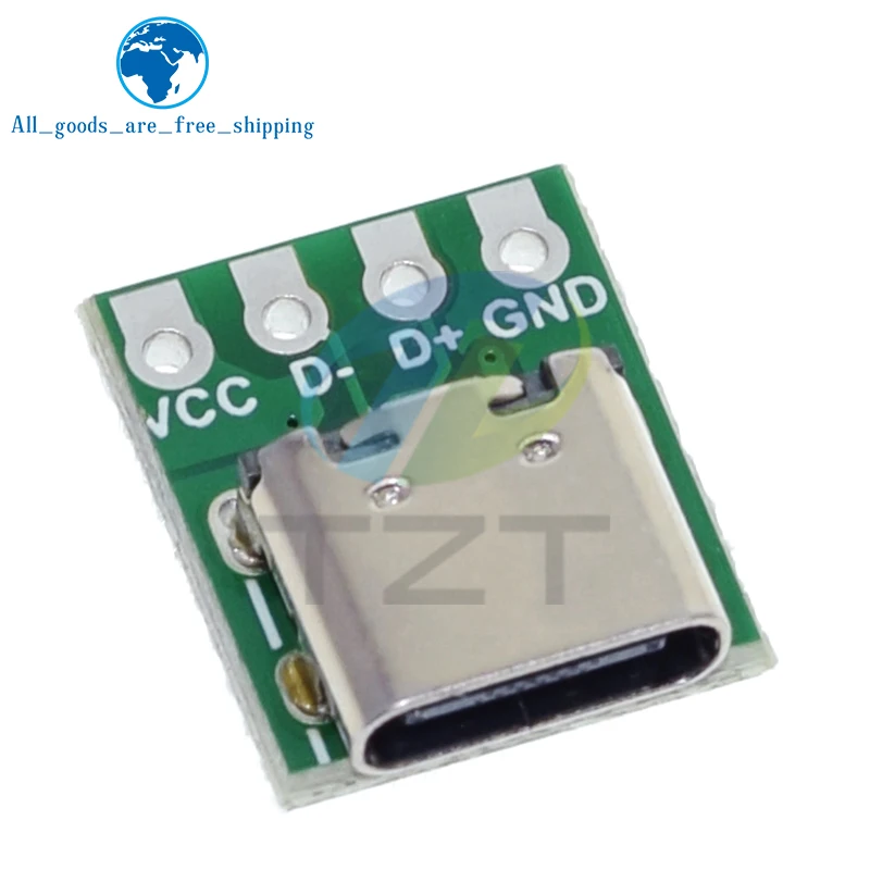
The physical design of the USB Type-C connector on this breakout board adheres to the standard reversible form factor. Its robust metal shell provides mechanical protection for the internal contacts, a common feature in modern USB-C implementations. The connector's inherent reversibility simplifies connection orientation.
This particular adapter breaks out a selection of 16 pins, specifically highlighting VCC, D-, D+, and GND. These are the core connections for basic power delivery and USB 2.0 data communication. The clear labeling on the PCB ensures straightforward identification of each pin.
Unlike fully integrated USB-C ports on consumer devices, which often present a complex array of 24 pins for advanced features like USB 3.1/3.2 data lanes, DisplayPort Alternate Mode, or Power Delivery (PD) negotiation, this board focuses on the most frequently utilized lines. This simplification reduces complexity for many common applications.
PCB Layout and Soldering Facilitation
Examination of the green printed circuit board (PCB) reveals a compact and functional layout. The board dimensions, approximately 13.30mm by 11.60mm, indicate its suitability for space-constrained projects. This is a small footprint.
The generously sized solder pads, clearly visible on the PCB, are crucial for reliable manual assembly. This design choice directly facilitates easier soldering, reducing the likelihood of cold joints or bridging, which are common issues in high-density surface-mount components. Unlike smaller, more delicate pads found on integrated components, these larger pads provide ample surface area for solder adhesion and tool access, making the board highly amenable to hand-soldering techniques even for those with moderate experience.
The through-hole design for the breakout pins offers superior mechanical stability compared to purely surface-mount pads for external connections. This robust connection point is vital for projects that might experience repeated plugging and unplugging of external wires or where physical stress on the connections is a concern. The board's simplicity is a significant advantage.
Signal Path Considerations and Electrical Integrity
The breakout of VCC, D-, D+, and GND pins directly addresses the fundamental requirements for USB 2.0 communication and basic power delivery. VCC provides the 5V power supply, while GND establishes the common electrical reference.
The D
For applications requiring higher data rates (e.g., USB 3.1 SuperSpeed), additional differential pairs (TX/RX) and CC (Configuration Channel) lines would be necessary. This board, by focusing on the USB 2.0 subset, streamlines its use for tasks that do not demand the full bandwidth of USB 3.1. Its purpose is clear.
Versatile Application Scenarios
This USB-C breakout board finds its primary utility in prototyping and repair. For instance, in a scenario where a device's internal USB-C port is damaged, this adapter can serve as a temporary or permanent external replacement, allowing the device to regain basic charging and data capabilities. This can save expensive equipment.
Electronics developers can integrate this board into custom projects, providing a standardized USB-C interface for power input or data exchange with microcontrollers and other embedded systems. Its compact size makes it ideal for integrating into custom enclosures or small form-factor devices. The board offers essential functionality.
Furthermore, for educational purposes, this breakout board offers a tangible way to understand the basic pinout and functionality of a USB-C connector without the complexity of a full 24-pin interface. Students can easily experiment with power delivery and basic data communication. It is an excellent learning tool.
Long-Term Viability and Value Proposition
The construction appears solid for its intended purpose. The metal shielding of the USB-C connector provides good physical durability against repeated insertions and extractions. This is a key aspect for longevity.
From a cost perspective, acquiring these breakout boards, especially in multi-packs, offers significant value for money. Instead of replacing an entire circuit board or device due to a damaged USB-C port, a technician can often repair the connection using this affordable component, extending the life of the equipment. This approach minimizes repair costs.
While the board focuses on USB 2.0 functionality, its core purpose is to provide a reliable, accessible interface. For projects or repairs that do not require the full suite of USB 3.1 features, this board represents an efficient and economical solution. Its utility is undeniable.
Imagine the satisfaction of restoring a beloved gadget to full functionality with a simple, precise repair, or the ease of integrating a modern USB-C interface into your custom electronics project without grappling with complex surface-mount soldering. This small board empowers both repair professionals and hobbyists to achieve reliable connectivity and extend the lifespan of their electronics, making advanced interfaces accessible and manageable.