USB 3.1 Type-C Breakout Board for Prototyping and Repair
Official Store Deal
Expert Analysis Overview
Precision in Prototyping: The Foundation of Connectivity
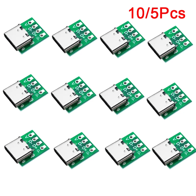
The USB 3.1 Type-C Breakout Board is a fundamental component for electronics enthusiasts and repair technicians, offering a robust and accessible interface for integrating modern USB-C connectivity into custom projects or for diagnostic purposes. This small, green printed circuit board (PCB) provides direct access to the essential pins of a USB Type-C connector, simplifying complex wiring tasks. Its design facilitates easy soldering for power and data lines. The board serves as a critical bridge for development.The visible design emphasizes direct access to key USB-C pins. Specifically, the board breaks out V (Voltage), D
For hobbyists and professional technicians, this layout means rapid prototyping and repair. Instead of attempting to solder directly to the tiny, closely spaced pins of a surface-mount USB-C connector on a main device, users can connect wires to these larger, more manageable pads. This significantly reduces the difficulty and risk of damaging the connector or the main board. It simplifies complex wiring. Compared to attempting direct soldering onto a device's main PCB, which often requires specialized equipment and high levels of precision, this breakout board offers a vastly simpler and safer alternative. Standard through-hole soldering techniques are sufficient. This approach minimizes the potential for short circuits or cold joints. It is a practical solution.
Architectural Integrity: Examining the PCB and Connector
The physical dimensions of the board are approximately 12mm by 13.8mm. This compact footprint allows for integration into tight spaces. The PCB itself is a standard green fiberglass substrate, commonly used in electronics for its durability and cost-effectiveness. The small size is advantageous.Such compact dimensions make these boards ideal for embedding into custom enclosures or for repairs where space is at a premium. The small form factor ensures that the added component does not significantly alter the device's original design or ergonomics. It fits almost anywhere. The visible traces appear clean and well-defined, suggesting a standard manufacturing process suitable for low-power data and charging applications. This indicates careful design.
Many generic breakout boards often feature flimsy construction or poorly aligned pads. This board, however, appears to offer a clean, functional layout. The metal housing of the USB-C connector itself provides a degree of mechanical resilience. It protects internal pins. This construction is reliable.
Signal Pathways: Ensuring Data and Power Flow
The exposed pins, V, D-, D+, and G, are fundamental for USB 2.0 communication and power delivery. The 'V' pad is for the 5V power supply, and 'G' is for ground. These are essential for powering small devices.For applications requiring basic data transfer and charging, these pins are all that are typically needed. The direct routing from the USB-C connector to the breakout pads minimizes signal path length. This helps in maintaining signal integrity for USB 2.0 data rates. Clean signals are crucial. Short paths reduce interference.
Unlike more complex USB-C breakout boards that might expose all 16 or 24 pins for USB 3.x or Thunderbolt functionalities, this board focuses on the most commonly used lines. This simplification reduces complexity and cost. It is a focused design. This makes it perfect for charging circuits or basic peripheral connections where high-speed data is not a requirement. Simplicity aids integration.
Integration Versatility: Beyond Basic Connections
The primary utility of these breakout boards lies in their versatility for repair and custom development. Technicians can use them to replace a damaged USB-C port on a smartphone, tablet, or other electronic device. This saves expensive equipment. It is a smart repair.Imagine a scenario where a laptop's USB-C charging port has failed due to physical stress. Instead of replacing the entire motherboard, which can be prohibitively expensive, a skilled technician can desolder the damaged port and wire in one of these breakout boards. This extends the life of the device. The cost savings are significant. This is a practical solution.
In contrast to simply discarding a device with a faulty port, these small components enable a sustainable repair strategy. They empower users to fix rather than replace. This reduces electronic waste. For custom projects, adding a modern USB-C interface to a microcontroller project or a DIY power bank becomes straightforward. New possibilities emerge.
Longevity and Reliability: A Technician's Perspective
The durability of the connection largely depends on the quality of the soldering and the mechanical strain applied to the final assembly. The metal shell of the Type-C connector provides good physical protection for the internal contacts. It resists wear. This enhances lifespan.Proper installation, including strain relief for any connected wires, will ensure long-term reliability. The robust nature of the PCB material itself means it will withstand typical handling during assembly and use. Cold joints must be avoided. Good soldering is key.
Many generic connectors can suffer from poor contact reliability over time. The standard Type-C connector, when properly integrated with a solid solder connection to this breakout board, should offer consistent performance. This ensures stable power and data. It is a dependable choice. Consistency is vital.
Value Proposition: Repair vs. Replacement
The product is offered in packs of 5 or 10 pieces. This bulk packaging provides excellent value for money. For a price point around $3.52 USD, acquiring multiple units makes economic sense. This reduces cost per unit. Bulk buying saves.For repair shops or active hobbyists, having a stock of these boards on hand means immediate access to a critical repair component. This eliminates downtime waiting for parts. The cost of a single board is negligible compared to the value of the device it can repair. It's an affordable fix. Readiness is an advantage.
Considering the alternative of replacing an an entire device or a complex mainboard due to a single damaged port, these breakout boards offer a clear return on investment. They are a cost-effective solution. This strategy aligns with both economic prudence and environmental responsibility. Repair makes sense.
The Technician's Toolkit Essential
These USB-C breakout boards are an indispensable addition to any electronics repair or prototyping toolkit. They simplify complex tasks, reduce repair costs, and promote device longevity. Their compact size and clear pinout make them highly adaptable. The value is clear.Imagine the satisfaction of successfully repairing a beloved gadget or bringing a custom project to life with reliable USB-C connectivity. These boards provide the foundation for countless electronic endeavors, ensuring stable power and data flow. They empower creation and repair. This small component opens up a world of possibilities for innovation and problem-solving, making advanced connectivity accessible to everyone. Your projects will thrive.