Universal SMD to DIP Adapter PCB Kit
Official Store Deal
Expert Analysis Overview
The Universal SMD to DIP Adapter PCB Kit is an indispensable collection of prototyping boards designed for electronics developers who regularly interface surface-mount devices (SMDs) with traditional through-hole breadboards and development platforms. This kit addresses the critical need for seamless integration, allowing modern, compact ICs to be utilized in more accessible, hand-solderable formats. As a certified electrician, the focus remains on ensuring robust electrical connections and preventing potential issues arising from improper component adaptation.
Modern electronics heavily rely on surface-mount technology (SMT) due to its efficiency in manufacturing and smaller form factors. However, this presents a significant challenge for hobbyists, students, and even professional engineers during the prototyping phase. Directly soldering fine-pitch SMD components onto perfboards or attempting to use them with standard breadboards is often impractical, leading to unreliable connections and potential damage. This adapter kit provides a structured solution.
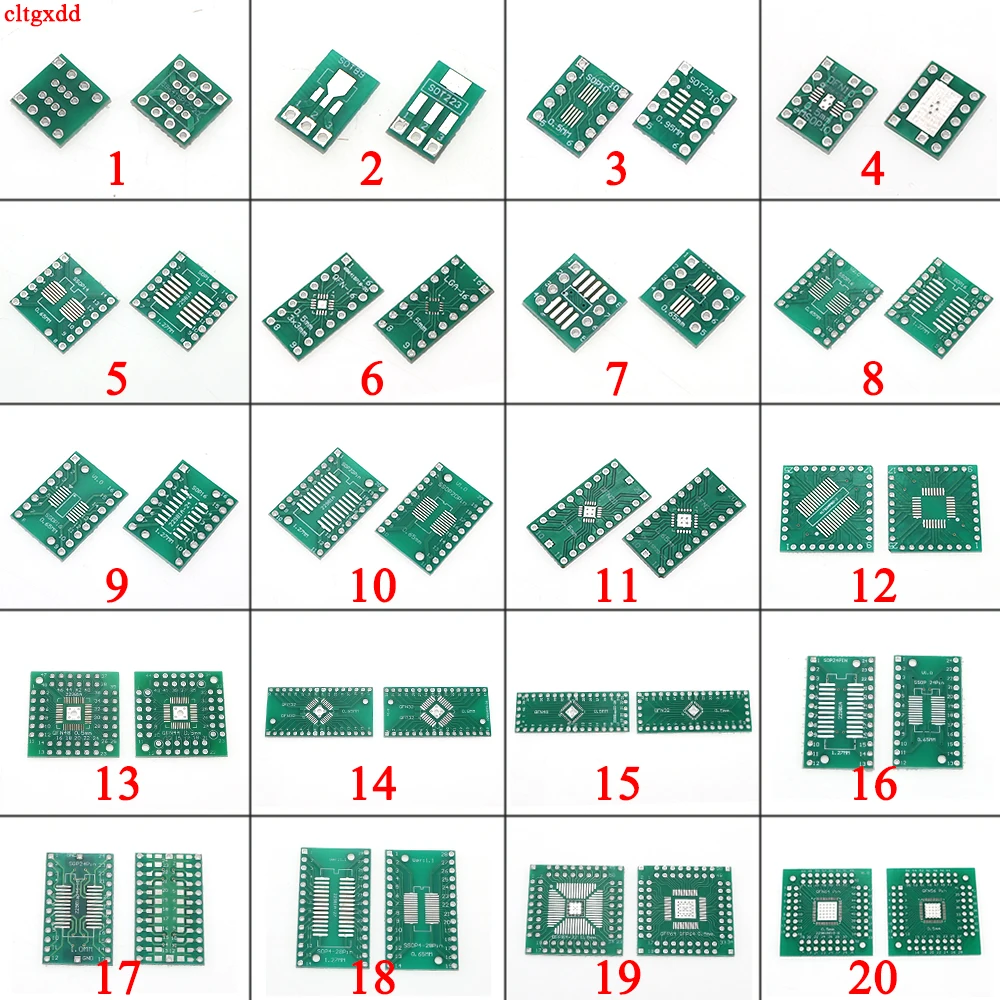
The visible components are small, green printed circuit boards (PCBs), each meticulously designed to convert a specific SMD package into a dual in-line package (DIP) footprint. This conversion is crucial. It allows for the easy insertion of complex integrated circuits into standard 2.54mm pitch breadboards, simplifying circuit development and testing. The frustration of incompatible footprints is eliminated.
Unlike makeshift solutions involving direct wire soldering or custom-fabricated boards for every single component, these pre-designed adapters offer a standardized, repeatable, and reliable interface. This approach significantly reduces the time and effort spent on mechanical adaptation, allowing more focus on circuit functionality. It is a fundamental tool for efficient development.
The comprehensive nature of this kit is immediately apparent from the visual input, showcasing a wide array of adapter types. The images clearly display boards for common SMD packages such as SOP8, SOP14, SOP16, SOP20, SOP24, SOP28, alongside TSSOP, QFP, SOT23, SOT89, and MSOP10. This extensive selection is a major advantage.
This broad compatibility ensures that developers are equipped to handle a vast majority of integrated circuits encountered in contemporary designs. Whether working with microcontrollers, operational amplifiers, or specialized communication chips, the likelihood of finding a suitable adapter within this kit is high. Engineers can adapt components quickly.
A generic adapter kit often provides only a limited selection of the most common packages, forcing users to purchase additional, specialized boards for less frequently used components. This comprehensive set, however, minimizes the need for multiple, fragmented purchases, offering a more complete and ready-to-use solution. It saves both time and money.
Many of the adapter boards featured in this kit exhibit a dual-sided design, a clever engineering choice that maximizes their utility. One side might accommodate a specific package pitch, while the reverse side offers compatibility with a different, often finer, pitch for the same or a similar package type. This design is highly practical.
This dual-sided approach effectively doubles the utility of each individual board, allowing for greater flexibility when working with components that come in slightly different variations of the same package. For instance, a single board might convert both a standard SOP package and its narrower SSOP counterpart. This reduces inventory needs.
Traditional single-sided adapters require a separate board for each pitch variation, leading to a larger, more cumbersome collection. The dual-sided design streamlines the prototyping process, making it easier to select the correct adapter without sifting through numerous options. It is an efficient use of space.
The physical construction of these adapter boards is a critical factor in their reliability and safety. The visible material appears to be standard FR-4 fiberglass laminate, a widely accepted substrate for printed circuit boards due to its excellent electrical and mechanical properties. This material choice is fundamental.
FR-4 provides a stable and rigid platform, preventing warping during the soldering process and ensuring consistent electrical performance. Its good dielectric properties minimize signal loss and crosstalk, which is essential for maintaining signal integrity, especially in sensitive analog or high-speed digital circuits. Proper insulation is key.
Inferior quality boards might utilize cheaper, less stable substrates that are prone to warping, delamination, or exhibit poor electrical characteristics. Such boards can compromise the reliability of the circuit and even pose safety risks if traces lift or short. These FR-4 boards offer a reliable foundation.
Each adapter board features clear and precise silkscreen markings, indicating pin numbers, component outlines, and sometimes even package names. These markings are not merely aesthetic; they serve a crucial functional purpose in preventing assembly errors. Accuracy is paramount.
These visual cues guide the user in correctly orienting the SMD component and connecting the appropriate header pins to the DIP side. Misaligning a component or incorrectly identifying a pin can lead to circuit malfunction or, more critically, permanent damage to the integrated circuit or other components. Verification is essential.
Without clear markings, users would rely solely on datasheets and careful counting, a process prone to human error, especially with fine-pitch components. The silkscreen acts as an immediate visual reference, significantly reducing the likelihood of costly mistakes during assembly. It simplifies complex tasks.
Successful adaptation hinges on the quality of the solder pads and the precision of their layout. The images reveal clearly defined solder pads, some accommodating very fine pitches such as 0.5mm, 0.65mm, 0.95mm, and 1.27mm. These dimensions are critical for modern SMDs.
Well-designed pads with appropriate solder mask clearance facilitate easier and more reliable soldering, even for components with extremely fine lead pitches. This design minimizes the risk of solder bridges forming between adjacent pins, which are a common cause of short circuits and component failure. Clean joints are vital.
Poorly designed pads, inconsistent plating, or inadequate spacing can make soldering a frustrating and error-prone experience, particularly for those new to SMD work. These boards, with their visible pad quality, aim to simplify the soldering process, promoting robust electrical connections. They enhance user experience.
While not explicitly detailed in the specifications, the visible traces on these adapter boards appear to be of adequate width for typical low-power prototyping applications. For a certified electrician, trace width directly correlates to current carrying capacity and potential for overheating. Trace integrity matters.
For most integrated circuits used in prototyping, which typically draw milliamps of current, the trace widths observed are generally sufficient to prevent excessive voltage drop or localized heating. However, for applications involving higher currents, such as power management ICs, careful consideration of the adapter's limitations is necessary. Always check current ratings.
Unlike custom-designed PCBs where trace widths can be precisely calculated for specific current loads, these universal adapters are designed for general-purpose use. Users should exercise caution and verify that the current requirements of their components do not exceed the implied capacity of the adapter's traces. Overloading can cause issues.
The product is offered as a 10-piece set at a highly competitive price point, making it an exceptionally cost-effective solution for anyone involved in electronics development. This bulk offering provides significant value. It is an investment in future project flexibility.
Acquiring a diverse set of these adapters at such an accessible price significantly lowers the barrier to entry for working with modern, compact integrated circuits. It allows hobbyists and educational institutions to experiment with advanced components without incurring prohibitive costs for specialized tools or custom PCBs. Budget-friendly development is possible.
Purchasing individual adapters for each specific IC package can quickly accumulate costs and lead to delays as different types are sourced. This comprehensive kit offers a ready-to-use, cost-effective bulk solution that ensures a suitable adapter is usually on hand when needed. It streamlines the procurement process.
As passive components, these adapter boards themselves do not pose inherent electrical hazards. However, their proper use is critical to the overall safety and reliability of the circuit being developed. The primary safety concern revolves around correct assembly and avoiding electrical shorts. Careful handling is required.
The clear silkscreen markings and the standardized 2.54mm DIP pin spacing on these boards significantly aid in preventing misconnections. Incorrect wiring or solder bridges can lead to short circuits, potentially damaging expensive integrated circuits, power supplies, or even creating localized heating that could pose a fire risk. Verifying connections before applying power is essential.
Compared to free-wiring SMD components directly onto perfboards, which increases the risk of accidental shorts and unreliable connections, these adapters provide a much more organized and predictable interface. This structured approach, when combined with careful soldering practices, contributes to a safer and more stable prototyping environment. They promote best practices.
Imagine a development process where the frustration of incompatible component packages is a distant memory. This adapter kit empowers rapid iteration and experimentation, allowing engineers and hobbyists to focus on the core functionality of their circuits rather than wrestling with physical component adaptation. The ability to quickly integrate a wide range of SMD components into a breadboard environment accelerates the entire design cycle. This means more time spent innovating and less time troubleshooting basic connectivity issues. The confidence derived from reliable, well-connected components translates into more robust and successful projects. This kit is a foundational element for any modern electronics workbench, enabling seamless transitions from concept to functional prototype with unparalleled ease and efficiency. It simplifies complex tasks, making advanced electronics accessible to all skill levels.
Bridging the Component Divide: The Necessity of Adapters
Modern electronics heavily rely on surface-mount technology (SMT) due to its efficiency in manufacturing and smaller form factors. However, this presents a significant challenge for hobbyists, students, and even professional engineers during the prototyping phase. Directly soldering fine-pitch SMD components onto perfboards or attempting to use them with standard breadboards is often impractical, leading to unreliable connections and potential damage. This adapter kit provides a structured solution.
The visible components are small, green printed circuit boards (PCBs), each meticulously designed to convert a specific SMD package into a dual in-line package (DIP) footprint. This conversion is crucial. It allows for the easy insertion of complex integrated circuits into standard 2.54mm pitch breadboards, simplifying circuit development and testing. The frustration of incompatible footprints is eliminated.
Unlike makeshift solutions involving direct wire soldering or custom-fabricated boards for every single component, these pre-designed adapters offer a standardized, repeatable, and reliable interface. This approach significantly reduces the time and effort spent on mechanical adaptation, allowing more focus on circuit functionality. It is a fundamental tool for efficient development.
Precision in Prototyping: Diverse Footprint Support
The comprehensive nature of this kit is immediately apparent from the visual input, showcasing a wide array of adapter types. The images clearly display boards for common SMD packages such as SOP8, SOP14, SOP16, SOP20, SOP24, SOP28, alongside TSSOP, QFP, SOT23, SOT89, and MSOP10. This extensive selection is a major advantage.
This broad compatibility ensures that developers are equipped to handle a vast majority of integrated circuits encountered in contemporary designs. Whether working with microcontrollers, operational amplifiers, or specialized communication chips, the likelihood of finding a suitable adapter within this kit is high. Engineers can adapt components quickly.
A generic adapter kit often provides only a limited selection of the most common packages, forcing users to purchase additional, specialized boards for less frequently used components. This comprehensive set, however, minimizes the need for multiple, fragmented purchases, offering a more complete and ready-to-use solution. It saves both time and money.
Dual-Sided Design for Enhanced Versatility
Many of the adapter boards featured in this kit exhibit a dual-sided design, a clever engineering choice that maximizes their utility. One side might accommodate a specific package pitch, while the reverse side offers compatibility with a different, often finer, pitch for the same or a similar package type. This design is highly practical.
This dual-sided approach effectively doubles the utility of each individual board, allowing for greater flexibility when working with components that come in slightly different variations of the same package. For instance, a single board might convert both a standard SOP package and its narrower SSOP counterpart. This reduces inventory needs.
Traditional single-sided adapters require a separate board for each pitch variation, leading to a larger, more cumbersome collection. The dual-sided design streamlines the prototyping process, making it easier to select the correct adapter without sifting through numerous options. It is an efficient use of space.
Ensuring Electrical Integrity: Material and Construction
The physical construction of these adapter boards is a critical factor in their reliability and safety. The visible material appears to be standard FR-4 fiberglass laminate, a widely accepted substrate for printed circuit boards due to its excellent electrical and mechanical properties. This material choice is fundamental.
FR-4 provides a stable and rigid platform, preventing warping during the soldering process and ensuring consistent electrical performance. Its good dielectric properties minimize signal loss and crosstalk, which is essential for maintaining signal integrity, especially in sensitive analog or high-speed digital circuits. Proper insulation is key.
Inferior quality boards might utilize cheaper, less stable substrates that are prone to warping, delamination, or exhibit poor electrical characteristics. Such boards can compromise the reliability of the circuit and even pose safety risks if traces lift or short. These FR-4 boards offer a reliable foundation.
Clear Silkscreen Markings for Error Prevention
Each adapter board features clear and precise silkscreen markings, indicating pin numbers, component outlines, and sometimes even package names. These markings are not merely aesthetic; they serve a crucial functional purpose in preventing assembly errors. Accuracy is paramount.
These visual cues guide the user in correctly orienting the SMD component and connecting the appropriate header pins to the DIP side. Misaligning a component or incorrectly identifying a pin can lead to circuit malfunction or, more critically, permanent damage to the integrated circuit or other components. Verification is essential.
Without clear markings, users would rely solely on datasheets and careful counting, a process prone to human error, especially with fine-pitch components. The silkscreen acts as an immediate visual reference, significantly reducing the likelihood of costly mistakes during assembly. It simplifies complex tasks.
The Solderability Factor: Pad Design and Pitch
Successful adaptation hinges on the quality of the solder pads and the precision of their layout. The images reveal clearly defined solder pads, some accommodating very fine pitches such as 0.5mm, 0.65mm, 0.95mm, and 1.27mm. These dimensions are critical for modern SMDs.
Well-designed pads with appropriate solder mask clearance facilitate easier and more reliable soldering, even for components with extremely fine lead pitches. This design minimizes the risk of solder bridges forming between adjacent pins, which are a common cause of short circuits and component failure. Clean joints are vital.
Poorly designed pads, inconsistent plating, or inadequate spacing can make soldering a frustrating and error-prone experience, particularly for those new to SMD work. These boards, with their visible pad quality, aim to simplify the soldering process, promoting robust electrical connections. They enhance user experience.
Trace Width and Current Handling
While not explicitly detailed in the specifications, the visible traces on these adapter boards appear to be of adequate width for typical low-power prototyping applications. For a certified electrician, trace width directly correlates to current carrying capacity and potential for overheating. Trace integrity matters.
For most integrated circuits used in prototyping, which typically draw milliamps of current, the trace widths observed are generally sufficient to prevent excessive voltage drop or localized heating. However, for applications involving higher currents, such as power management ICs, careful consideration of the adapter's limitations is necessary. Always check current ratings.
Unlike custom-designed PCBs where trace widths can be precisely calculated for specific current loads, these universal adapters are designed for general-purpose use. Users should exercise caution and verify that the current requirements of their components do not exceed the implied capacity of the adapter's traces. Overloading can cause issues.
Value for the Development Bench: Cost-Effectiveness and Accessibility
The product is offered as a 10-piece set at a highly competitive price point, making it an exceptionally cost-effective solution for anyone involved in electronics development. This bulk offering provides significant value. It is an investment in future project flexibility.
Acquiring a diverse set of these adapters at such an accessible price significantly lowers the barrier to entry for working with modern, compact integrated circuits. It allows hobbyists and educational institutions to experiment with advanced components without incurring prohibitive costs for specialized tools or custom PCBs. Budget-friendly development is possible.
Purchasing individual adapters for each specific IC package can quickly accumulate costs and lead to delays as different types are sourced. This comprehensive kit offers a ready-to-use, cost-effective bulk solution that ensures a suitable adapter is usually on hand when needed. It streamlines the procurement process.
Mitigating Prototyping Risks: Safety and Reliability
As passive components, these adapter boards themselves do not pose inherent electrical hazards. However, their proper use is critical to the overall safety and reliability of the circuit being developed. The primary safety concern revolves around correct assembly and avoiding electrical shorts. Careful handling is required.
The clear silkscreen markings and the standardized 2.54mm DIP pin spacing on these boards significantly aid in preventing misconnections. Incorrect wiring or solder bridges can lead to short circuits, potentially damaging expensive integrated circuits, power supplies, or even creating localized heating that could pose a fire risk. Verifying connections before applying power is essential.
Compared to free-wiring SMD components directly onto perfboards, which increases the risk of accidental shorts and unreliable connections, these adapters provide a much more organized and predictable interface. This structured approach, when combined with careful soldering practices, contributes to a safer and more stable prototyping environment. They promote best practices.
The Future of Prototyping: Streamlined Development
Imagine a development process where the frustration of incompatible component packages is a distant memory. This adapter kit empowers rapid iteration and experimentation, allowing engineers and hobbyists to focus on the core functionality of their circuits rather than wrestling with physical component adaptation. The ability to quickly integrate a wide range of SMD components into a breadboard environment accelerates the entire design cycle. This means more time spent innovating and less time troubleshooting basic connectivity issues. The confidence derived from reliable, well-connected components translates into more robust and successful projects. This kit is a foundational element for any modern electronics workbench, enabling seamless transitions from concept to functional prototype with unparalleled ease and efficiency. It simplifies complex tasks, making advanced electronics accessible to all skill levels.