Precision Solder Pad Repair Sheet for Mobile Motherboards
Official Store Deal
Expert Analysis Overview
The Precision Solder Pad Repair Sheet is a highly specialized, budget-conscious solution engineered for intricate mobile phone motherboard repairs, targeting technicians and advanced hobbyists. This product directly addresses the common challenges associated with damaged solder pads and broken traces, offering a streamlined alternative to traditional flywiring techniques. Its design focuses on delivering clean, stable, and aesthetically superior repairs, making it an essential addition to a compact, organized toolkit for those who frequently tackle micro-soldering tasks. The sheet provides a definitive upgrade in repair methodology. It is a critical component for modern electronics maintenance. This item facilitates intricate work.
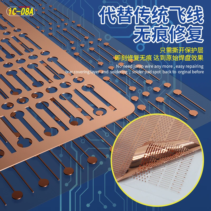
Traditional methods for repairing damaged solder pads or broken traces on printed circuit boards often involve tedious flywiring. This process requires precise soldering of thin wires to bridge connections, which can be time-consuming, aesthetically unpleasing, and prone to future failures if not executed perfectly. The images clearly depict the product's fundamental purpose: to replace this laborious flywire method. The sheet itself presents a grid of pre-formed copper pads. These pads are designed for quick application.
This solder pad repair sheet fundamentally redefines the approach to micro-repairs. Instead of manually bending and soldering delicate wires, users can select a pre-shaped copper pad, adhere it, and solder directly onto it. This significantly reduces the complexity and skill barrier for achieving professional-grade results. The visible array of pad shapes and sizes suggests broad applicability. It enhances repair efficiency. This stands in stark contrast to the often inconsistent and bulky results of hand-soldered flywires, which can introduce new points of failure or make future diagnostics more difficult.
Compared to generic repair kits that might offer only basic tools or rudimentary materials, this specialized sheet provides a targeted solution. It focuses on a specific, common problem in electronics repair. The product's explicit aim is to deliver a 'traceless repair,' implying a finish that closely mimics the original circuit board design. This is a considerable advantage over improvisational repair techniques. It saves time and effort.
The product description highlights the use of industrial-grade printed circuit board copper foil with a thickness of 30μm. This specific material choice is crucial for both electrical performance and mechanical durability. Copper, renowned for its excellent electrical conductivity, ensures that repaired connections maintain optimal signal integrity, which is paramount for sensitive electronic devices like mobile phones. The material's quality is visible.
The 30μm thickness strikes a balance between flexibility and robustness. It is thin enough to conform to the contours of a motherboard but substantial enough to provide a strong, reliable electrical path. This precise thickness prevents the pads from being too flimsy, which could lead to accidental damage during handling or soldering, or too thick, which might create an uneven surface. Such material specifications are not arbitrary. They are engineered for purpose. This ensures longevity for the repair.
Standard repair foils or makeshift solutions often fall short in material quality. Many generic alternatives might use thinner, less conductive, or less durable materials, leading to repairs that are temporary or degrade quickly. The industrial-grade copper foil in this product offers a superior alternative, providing a repair that is not only functional but also built to last. It resists corrosion effectively. This commitment to quality translates directly into more reliable device operation post-repair.
The application process for these solder pads is designed for efficiency and ease, as suggested by the visual instructions. The user simply needs to peel off a protective layer, position the appropriate pad over the damaged area, and then solder it into place. This simplifies complex tasks. The inclusion of an adhesive backing further streamlines the process, holding the pad securely while soldering. This prevents movement and ensures precise alignment.
One of the key advantages is the variety of pad shapes and sizes available on a single sheet. The images clearly show an assortment of circular, oval, and elongated pads, indicating compatibility with diverse component footprints and trace configurations found on mobile phone motherboards. This versatility means technicians don't need multiple specialized tools. It covers many repair scenarios. This broad compatibility reduces the need for custom fabrication of repair points.
Compared to the intricate hand-sculpting of solder masks or the delicate placement of tiny wires, this pre-fabricated pad system significantly lowers the barrier to entry for complex repairs. It allows even less experienced users to achieve results typically associated with advanced soldering skills. The direct application saves valuable time. This makes the repair process more accessible to a wider range of users, from seasoned professionals to enthusiastic DIYers.
One of the product's central claims is its ability to facilitate a 'traceless repair.' This refers to the aesthetic outcome where the repaired area seamlessly integrates with the existing circuit board, leaving minimal visual evidence of the intervention. The before-and-after images provide compelling evidence of this capability, showing damaged pads restored to a near-original appearance. This is a significant improvement.
The ability to fix the pad and then cover it with green oil (UV curing solder mask ink) further enhances the repair's integrity and visual appeal. Applying a solder mask over the repaired area provides additional insulation, protects against environmental factors like moisture and dust, and restores the board's original protective layer. This step is crucial for long-term durability. It ensures a professional finish.
In contrast, traditional flywire repairs often leave visible wires and solder joints that can look messy and unprofessional. These exposed elements are also more vulnerable to physical damage or short circuits. The solder pad repair sheet offers a superior alternative, not just in functionality but also in maintaining the device's original aesthetic and protective qualities. It is a cleaner method. This attention to detail reflects a higher standard of repair.
For a first-time renter, or any budget-conscious individual, the economic implications of device repair are significant. Replacing a mobile phone, especially a flagship model, represents a substantial financial outlay. This solder pad repair sheet offers a cost-effective solution for extending the life of valuable electronics. It avoids costly replacements. The initial investment in this repair kit is minimal compared to the price of a new device or professional repair services.
By enabling users to perform intricate repairs themselves, the product provides a substantial return on investment (ROI). It transforms a potentially expensive problem into an manageable DIY project. This capability empowers users to save money and reduce electronic waste, aligning with a more sustainable approach to consumption. The value proposition is clear. It fosters self-sufficiency.
When considering a compact toolkit for a new apartment, including items that offer practical cost savings is wise. This repair sheet fits perfectly into that philosophy, offering a high-capability solution without requiring a large, specialized workspace. Its compact nature makes it ideal for small living spaces. It is an intelligent purchase. This tool set offers significant long-term value.
While explicitly marketed for mobile phone motherboards, the inherent design of these solder pads suggests broader applicability. The variety of shapes and sizes, described as suitable for
The Evolution of Micro-Repair Techniques
Traditional methods for repairing damaged solder pads or broken traces on printed circuit boards often involve tedious flywiring. This process requires precise soldering of thin wires to bridge connections, which can be time-consuming, aesthetically unpleasing, and prone to future failures if not executed perfectly. The images clearly depict the product's fundamental purpose: to replace this laborious flywire method. The sheet itself presents a grid of pre-formed copper pads. These pads are designed for quick application.
This solder pad repair sheet fundamentally redefines the approach to micro-repairs. Instead of manually bending and soldering delicate wires, users can select a pre-shaped copper pad, adhere it, and solder directly onto it. This significantly reduces the complexity and skill barrier for achieving professional-grade results. The visible array of pad shapes and sizes suggests broad applicability. It enhances repair efficiency. This stands in stark contrast to the often inconsistent and bulky results of hand-soldered flywires, which can introduce new points of failure or make future diagnostics more difficult.
Compared to generic repair kits that might offer only basic tools or rudimentary materials, this specialized sheet provides a targeted solution. It focuses on a specific, common problem in electronics repair. The product's explicit aim is to deliver a 'traceless repair,' implying a finish that closely mimics the original circuit board design. This is a considerable advantage over improvisational repair techniques. It saves time and effort.
Material Science and Structural Integrity
The product description highlights the use of industrial-grade printed circuit board copper foil with a thickness of 30μm. This specific material choice is crucial for both electrical performance and mechanical durability. Copper, renowned for its excellent electrical conductivity, ensures that repaired connections maintain optimal signal integrity, which is paramount for sensitive electronic devices like mobile phones. The material's quality is visible.
The 30μm thickness strikes a balance between flexibility and robustness. It is thin enough to conform to the contours of a motherboard but substantial enough to provide a strong, reliable electrical path. This precise thickness prevents the pads from being too flimsy, which could lead to accidental damage during handling or soldering, or too thick, which might create an uneven surface. Such material specifications are not arbitrary. They are engineered for purpose. This ensures longevity for the repair.
Standard repair foils or makeshift solutions often fall short in material quality. Many generic alternatives might use thinner, less conductive, or less durable materials, leading to repairs that are temporary or degrade quickly. The industrial-grade copper foil in this product offers a superior alternative, providing a repair that is not only functional but also built to last. It resists corrosion effectively. This commitment to quality translates directly into more reliable device operation post-repair.
Streamlined Application and User Accessibility
The application process for these solder pads is designed for efficiency and ease, as suggested by the visual instructions. The user simply needs to peel off a protective layer, position the appropriate pad over the damaged area, and then solder it into place. This simplifies complex tasks. The inclusion of an adhesive backing further streamlines the process, holding the pad securely while soldering. This prevents movement and ensures precise alignment.
One of the key advantages is the variety of pad shapes and sizes available on a single sheet. The images clearly show an assortment of circular, oval, and elongated pads, indicating compatibility with diverse component footprints and trace configurations found on mobile phone motherboards. This versatility means technicians don't need multiple specialized tools. It covers many repair scenarios. This broad compatibility reduces the need for custom fabrication of repair points.
Compared to the intricate hand-sculpting of solder masks or the delicate placement of tiny wires, this pre-fabricated pad system significantly lowers the barrier to entry for complex repairs. It allows even less experienced users to achieve results typically associated with advanced soldering skills. The direct application saves valuable time. This makes the repair process more accessible to a wider range of users, from seasoned professionals to enthusiastic DIYers.
Repair Integrity and Visual Appeal
One of the product's central claims is its ability to facilitate a 'traceless repair.' This refers to the aesthetic outcome where the repaired area seamlessly integrates with the existing circuit board, leaving minimal visual evidence of the intervention. The before-and-after images provide compelling evidence of this capability, showing damaged pads restored to a near-original appearance. This is a significant improvement.
The ability to fix the pad and then cover it with green oil (UV curing solder mask ink) further enhances the repair's integrity and visual appeal. Applying a solder mask over the repaired area provides additional insulation, protects against environmental factors like moisture and dust, and restores the board's original protective layer. This step is crucial for long-term durability. It ensures a professional finish.
In contrast, traditional flywire repairs often leave visible wires and solder joints that can look messy and unprofessional. These exposed elements are also more vulnerable to physical damage or short circuits. The solder pad repair sheet offers a superior alternative, not just in functionality but also in maintaining the device's original aesthetic and protective qualities. It is a cleaner method. This attention to detail reflects a higher standard of repair.
Economic Value for the First-Time Renter
For a first-time renter, or any budget-conscious individual, the economic implications of device repair are significant. Replacing a mobile phone, especially a flagship model, represents a substantial financial outlay. This solder pad repair sheet offers a cost-effective solution for extending the life of valuable electronics. It avoids costly replacements. The initial investment in this repair kit is minimal compared to the price of a new device or professional repair services.
By enabling users to perform intricate repairs themselves, the product provides a substantial return on investment (ROI). It transforms a potentially expensive problem into an manageable DIY project. This capability empowers users to save money and reduce electronic waste, aligning with a more sustainable approach to consumption. The value proposition is clear. It fosters self-sufficiency.
When considering a compact toolkit for a new apartment, including items that offer practical cost savings is wise. This repair sheet fits perfectly into that philosophy, offering a high-capability solution without requiring a large, specialized workspace. Its compact nature makes it ideal for small living spaces. It is an intelligent purchase. This tool set offers significant long-term value.
Versatility Across Electronic Devices
While explicitly marketed for mobile phone motherboards, the inherent design of these solder pads suggests broader applicability. The variety of shapes and sizes, described as suitable for